Saturday, October 14, 2006

Can PLL self-locked without "External" input?

I was busy working on something and suddenly a crazy idea came up.


Can a PLL lock itself if I connect a PLL output clock to the PLL input clock on a PCB and both the PLL multiplication and division value is set to 1? I expected the answer is no, of course. But the curiosity kills sometimes. So, I went ahead and did the simple test.

I was using a Cyclone II device. Surprisingly, I saw the PLL locked output signal went high. However, the output signal frequency wasn't the expected frequency (10MHz). I probed at the PLL output clock (which was also connected to the PLL input clock signal), it showed about 420kHz.

So, what is the conclusion of this story? Nothing.

Saturday, September 02, 2006

Lattice Now Blogs!

Insteresting! Lattice now blogs! A lots of non-confidential-but-technical information out there!
It is always nice to see a FPGA vendor takes initiative to provide a platform for their knowledgable engineers to share their experience and knowledge. The good thing is that the knowledge shared is not only limited to Lattice products but all the vendors FPGA.
I know it is not easy for the writers as they now have one more repeatitive task in their long to-do list besides their daily jobs. Anyway, I hope they continue doing this! Bravo to all the writers!

Tuesday, August 01, 2006

Embed Tclet in Your HTML

Since started this blog, I found out that I need to study a minimum amount of HTML to display my writing correctly. Besides, I can have more control writing in "HTML mode" compared with "Compose mode". For an example, you can't just type the symbol "<" in your blog message, instead, you need to type "&lt;" to display "<" in your blog. Don't get me wrong, I am not trying to show off my HTML skills. In fact, I only have very basic and minimum knowledge about HTML.

Anyway, if I am not wrong (considering myself not a webmaster), it seems like HTML alone doesn't have the ability to let you do real-time programming stuff on your web browser, such as Mozilla Firefox or Internet Explorer. However, it can be done using a plugin.

There are many different types of plugins out there, but I choose to use Tcl applet or Tclet since I did some study on this language before. (If you've never heard of the Tcl/Tk language before, you can visit here.) I don't know how to embed a Tclet properly in blogspot. However, I manage to do it on another free site. This Tclet in this free site is to display all the gray code counter results in sequence after you have entered the number of bits your gray code counter is. I don't know how useful it is to you, but it is useful to me because I always forget how the gray code counter increments. Bear in mind that if you are a first-time user or viewer, you need to download and install the Tcl Web Browser Plugin for free. And, of course, it is SAFE to be installed in your PC. If you haven't installed it yet, you will see a blank square instead of the picture on the left side here.

It will be a bit long for me to describe how to embed Tclet in your HTML code here. The best source is the reference book that I show in here. Of course, you can look at the HTML code in the example above. Plenty of funky Tclet examples can also be easily found on web if you are interested to see others. Hope you like it.

Thursday, July 13, 2006

Save More Power In Handheld Devices


How to save more power when your CPLD device is in idle mode?
Use a very slow clock to reduce toggle rate? Partially disabling the logic inside the device? Well, why not powering off the device?
I came across this interesting article by accident and found it a simple yet smart idea to prolong the battery life of a portable handheld devices. In future, if I have the chance to design a portable product with interactive user interface, this idea will surely be the first one to cross my mind.
If for whatever reason, you have to use a FPGA in a battery-operated product, this article will sure help you more.

Sunday, July 02, 2006

OP-AMP Configurations Recall

It has been a while since I last dealed with op-amp. So, it is good to recall some of the most fundamental op-amp configurations, especially when I am dealing with them recently.
In my opinion, op-amp is like logic gates in analog world. You need op-amps to transfer your analog inputs into your desired analog outputs.
The following are some important notes for me, not for you, of course, :)!


Common NamesOp-Amp CircuitsTransfer Functions
Voltage Follower AmplifierVout = Vin
Inverting AmplifierVout = -(Rf/Rs)Vin
Noninverting AmplifierVout = (1+R2/R1)Vin
Difference AmplifierIf R1/R2 = R3/R4,
Vout = (Vin+ - Vin-)(R2/R1) + Vshift
Summing AmplifierVout = (R2/R1)* (V1+V2-V3-V4)

Sunday, June 04, 2006

Embedded Logic Analyzer inside FPGA


There is no reason to doubt that most of the FPGA users like you and me have gone through some painful experiences wanting to know what is happening inside an FPGA. It is even more painful when you strongly believe your code is working fine and you don’t have any clue which part of the design is causing you sleepless nights. You keep on routing all the suspected internal signals to the very limited unused I/O pins of your FPGA and then probe and trigger them on your oscilloscope that usually has only four channels or LESS! Sad to say, the oscilloscope couldn’t help much in situation like this unless it is related to the signal integrity issue.

If you are lucky, you can have a logic analyzer instrument to sample a lot of signals for your analysis and verification. Well, if you are not, good news for you, you can insert an embedded logic analyzer inside your FPGA and it is totally licensed-free, at least for Altera FPGA users! The Altera Embedded Logic Analyzer tool named SignalTap II is FREE for use even you don’t purchase any software license from Altera. That means you can use your SignalTap II inside Quartus II Web Edition software for FREE provided that you install and enable the TalkBack Feature of Quartus II software.


The SignalTap II works almost like a logic analyzer equipment but at a very much smaller scale as it has very limited on-chip memory to store the sampled data. Other logic analyzer’s features such as Rising-Edge triggering, Falling-Edge triggering, Either-Edge triggering, Boolean triggering, Multi-Level triggering and others are also available in the SignalTap II tool. In fact, you can also instantiate up to 127 SignalTap II instances in your design, as long as it can fit in your chosen FPGA device. You can imagine each instance of SignalTap II is a small scale of logic analyzer equipment which also has an external trigger-in and trigger-out. And, the input of the trigger-in can come from other instances trigger-out or I/O pins or any internal logic signal. I think this is an advantage to the SignalTap II because a logic analyzer equipment trigger-in must come from one of your device I/O pins, isn’t it? Anyway, I rarely make use of the trigger-in, trigger-out and the multiple analyzer features because I prefer to monitor all my signals in just one analyzer. Why bother creating so many instances of analyzer where it doesn’t help saving you any logic and memory resource at all? One of the reasons is you need to have different acquisition clocks for the signals that you are interested to tap. It could also be you have different sample depth requirement for your acquiring signals and etc.

The purpose of this post is not to teach you using SignalTap II, but to make you aware of the availability of this tool if you haven’t come across or heard of this tool. My life as a FPGA user would have been a lot easier if I learnt to use this tool immediately after learning Quartus II. Instead, I only had the chance to pick up this tool after about one year being an Altera user. It is worth every moment to learn and pick up this tool as it makes your debugging process simpler and a lot faster. Unlike Xilinx’s ChipScope Pro, you don’t need to install the SignalTap II tool separately. It comes together with Quartus II and it is available after the Quartus II installation is done.

Last but not least, thanks to Altera that the SignalTap II is FREE!!

Friday, May 19, 2006

USB-Blaster vs Platform Cable USB


Both USB-Blaster and Platform Cable USB are the USB download cables provided by Altera and Xilinx, respectively. Most of time, the download cable is a necessity while developing and debugging your design in the FPGA. You need them to download the FPGA configuration bitstream through JTAG or Passive/Slave serial mode, to program the CPLD, to program the configuration device, to download your firmware into the soft processor and to tap the signals inside the FPGA through the FPGA embedded logic analyzer. Both of them are able to achieve all the above-mentioned purposes. But what is the main difference between them? The SELLING PRICE!!! The USB-Blaster costs USD$300 while the Platform Cable USB only costs half the price of the USB-Blaster, which is USD$149. This is really killing me because sometimes I need to use more than one download cable at the same time when dealing with multi-FPGA environment. Why can’t the Altera USB-Blaster at least cost the same like the Xilinx Platform Cable USB? In fact, Xilinx Platform Cable USB has even more features than USB-Blaster such as programming the configuration clock frequency. The USB-Blaster operates at USB full speed, which is 12Mbps, while the Platform Cable USB can operate at USB high speed!

Frankly speaking, the download cable should cost as cheap as possible by the FPGA vendors because they should be making money from selling their FPGA and CPLD devices, not from selling the download cables. Similar to the Quartus II and ISE web edition software tool, the download cable should just be a marketing tool to help promote the usage of FPGA or CPLD solutions! Imagine if I am a newbie who want to learn to use FPGA or CPLD on my own, it doesn’t make sense for me to buy a tool that is much much more expensive than a single low-cost FPGA/CPLD device.

Anyway, just for your reference, I also compare the cost of download cables that use the PC parallel port interface which are Altera ByteBlaster II, USD$150 and Xilinx Parallel Cable IV, USD$95. Once again, Xilinx is the winner when it comes to the price war. Is this the reason Xilinx being the market leader? Well, you know better.

/////////////////////////////////////////////////////////////////////////////////
// Disclaimer: All the price stated above are extracted from Altera Buy On-Line and Xilinx Online Store websites at the posting time and may change from time to time in future.

Friday, May 05, 2006

Convert Floating Point to String

A few months ago, I found out that there is no built-in function for converting a floating point data type variable to a string although there are functions that do the following:

1. Convert a string to floating point (atof)
2. Convert an integer to string (itoa)
3. Convert a string to an integer (atoi)

All the above functions come in very handy when you want to write your data to a text file. It is quite intriguing because itoa(), atoi() and atof() are provided but ftoa() are not. Unfortunately, many data are floating points in nature. Also, data that are larger than a 32-bit integer are usually represented as floating point data type. Anyway, many programming experts have already provided ftoa() solution on their websites. I believe it is not difficult to find one out there but I would like to have my very own one, too, as it is no harm trying. The C/C++ code is as shown below. I have tested it in the Microsoft Visual C++ compiler but I do not cover all the possible cases. So, use it on your own risk. It is not the best solution available for ftoa() but it certainly enough to meet my purposes. If you need one, I hope that it helps you, as well. If not, you can always write one for yourself.


////////////////////////////////////////////////////////////////
// my_ftoa.cpp
// date created: May 5, 2006
// author:
http://fpgaforum.blogspot.com/
////////////////////////////////////////////////////////////////


#include <iostream>
#include <cmath>
using namespace std;
#define PRECISION_POINT 4 //Change this to display more or less precision point

void ftoa(float f, char* a, int point); //function prototype

void main()
{
  float f = -1.23456;
  char result[32];
  ftoa(f,result, PRECISION_POINT);
  cout << result;
}

void ftoa(float f, char* a, int point)
{
  char buf_int [2]; //temporary buffer
  char buf_d [16]; //to store the integral part, e.g. "-123" for "-123.456"
  char buf_f [16]; //to store all the fraction part, e.g. "000123" for "1.000123"
  char buf_nz [16]; //to store the non-zero fraction part, e.g. "123" for "1.000123"
  int d= (int)(f); //integral part

  float fp = (f<0) ? (d-f) : (f-d); //fractional part

  int fp2int = fp*(pow(10,point));
  int fpplus1 = fp*(pow(10,point+1));

  if((fpplus1%10)>=5)
    fp2int++;

  strcpy(buf_int,"");
  strcpy(buf_d,""); //clear the buffer, just to be safe
  strcpy(buf_f,""); //clear the buffer, just to be safe
  
strcpy(buf_nz,""); //clear the buffer, just to be safe

  if((d == 0) && (f<0) && (f>-1))
  {
    strcat(buf_d,"-");
    itoa(d,buf_int,10);
    strcat(buf_d,buf_int);
  }
  else
  {
    itoa(d,buf_d,10);
  }
  strcat(buf_d,".");
  //looking for the leading zeros at the fractional part
  if(fp2int == 0)
  {
    for(int i = 0; i < point-1; i++)
      strcat(buf_f,"0");
  }
  else if(fp2int < (pow(10,point-1)))
  {
    for(int i = 0; i < point; i++)
    {
      int j = pow(10,(point-1-i));
      if(fp2int < j)
        strcat(buf_f,"0");
      else break;
    }
  }

  itoa(fp2int,buf_nz,10);
  strcat(buf_f,buf_nz);
  strcat(buf_d,buf_f);
  strcpy(a,buf_d);
}

// The end
////////////////////////////////////////////////////////////////

Friday, April 21, 2006

Tcl Script to Automate Quartus II Compilation

Below is a sample Tcl script that I use to automate the compilation of my Quartus II projects overnight or over the weekend. You can easily find more information about the usage by just typing "tcl" on the Altera search column in www.altera.com and you can easily get some examples over there. The most relevant reading material for Quartus II tool specific scripts would be the Tcl Scripting chapter of the Quartus II Handbook.


############################################
## auto_compile.tcl
## date created : April 9, 2006
## author : http://fpgaforum.blogspot.com
############################################


###Assume that the objective of this script is to compile
###a similar project twice, one with a minimum current strength
###and the other with a maximum current strength.
###(Sometimes you need to do some characterization of the current
###strength on your hardware!)
###The final product is two sof files, one for the minimum
###current strength and the other one for the maximum
###current strength. This means that this script will also rename
###the sof file for after every compilation to avoid being overwritten
###on the next compilation cycle

###go to project folder in command prompt
### Then type quartus_sh -s
### Verify the Quartus II Version number is as targeted, if you have multiple
### versions of Quartus II on your PC
### After verified, type the following command:
### source (This filename.tcl)
### OR
### Open the Quartus II project, then open up the Quartus II Tcl Console by
### go to View->Utility Windows->Tcl Console
### In the Quartus II Tcl Console, type the following command if the tcl script
### is placed in the project folder:
### source (This filename.tcl)

########## TCL script starts #################

####### Auto Compilation TCL Script ############
#change the following line according to your Quartus II project folder##
##assume the 1st project that I want to compile is in the following folder
cd D:/data/project1

##This is to set the minimum current strength
set project_name project1
set revision_name project1
project_open -revision $revision_name $project_name;
set_global_assignment -name Family StratixII
set_global_assignment -name DEVICE EP2S60F1020C3ES

#some assignments to the pins. Of course, I am not going to list all
set_instance_assignment -name CURRENT_STRENGTH_NEW "MINIMUM CURRENT" -to data_bus[0]
set_instance_assignment -name CURRENT_STRENGTH_NEW "MINIMUM CURRENT" -to data_bus[1]

load_package flow
execute_flow -compile
project_close

set sof [pwd]/project1.sof
if [file exists $sof] {
file rename $sof project1_MIN.sof
} else {
puts "ERROR! RENAME $sof to project1_MIN.sof"
}

###======================================

##This is to set the maximum current strength
set project_name project1
set revision_name project1
project_open -revision $revision_name $project_name;
set_global_assignment -name Family StratixII
set_global_assignment -name DEVICE EP2S60F1020C3ES

#some assignments to the pins. Of course, I am not going to list all
set_instance_assignment -name CURRENT_STRENGTH_NEW "MAXIMUM CURRENT" -to data_bus[0]
set_instance_assignment -name CURRENT_STRENGTH_NEW "MAXIMUM CURRENT" -to data_bus[1]

load_package flow
execute_flow -compile
project_close

set sof [pwd]/project1.sof
if [file exists $sof] {
file rename $sof project1_MAX.sof
} else {
puts "ERROR! RENAME $sof to project1_MAX.sof"
}

###======================================
########## TCL script ends #################

Wednesday, April 19, 2006

The Secret of NIOS II Success


Altera NIOS II soft processor has been known as the world’s most versatile embedded processors. What is the reason behind since in my opinion the CPU architecture is more or less the same compared with other processors? In my opinion, the unsung hero that contributes to the success of the NIOS II processor is the Avalon Switch Fabric. I find it a bit weird that Altera or distributors does not put very much effort in directly marketing the Avalon Interface Specification introduced by Altera years ago. I strongly believe that the user-friendly Avalon Interface is one of the main reasons engineers choosing NIOS II processor over their main rival’s Xilinx MicroBlaze processor. It doesn’t matter whether you are designing a master or slave peripheral, as long as your own-designed peripheral supports Avalon Interface, your peripheral can communicate with others peripheral, including NIOS II processor flawlessly as the Avalon Switch Fabric will handle the communication for you.

The Avalon Switch Fabric is generated by Altera SOPC Builder that comes together with Quartus II software tool. That means after installing Quartus II, you do not need to worry about installing the SOPC Builder as it is part of Quartus II software. I like this because I don’t like to open a few application softwares at the same time doing one job. Another good point to mention about the SOPC Builder is the evaluation is free and valid for unlimited period. You just have to re-apply a new Quartus II web edition license about every three months through internet and the license will be sent to your email in split seconds. Too bad that the newly-announced NIOS II C-to-Hardware Acceleration (C2H) Compiler is not available for evaluation to the public without going through the Altera distributors. I am very curious with the improvement achieved using the C2H compiler.

Although many free peripherals that support Avalon interface are available, such as SDRAM controller, DDR SDRAM controller, interval timer, DMA module, UART, etc, it is still very critical to be able to connect your custom IP to the Avalon Switch Fabric. You will find yourself in a situation at times where you need to complete a lot of intensive calculation work within a very short period of time in FPGA. Some good examples are carrying out blemish test for a camera module and CRC checking for a large amount of data. Most of the time, the intensive calculation part takes too much time in C and therefore you can design your own IP in HDL to achieve the performance needed. The purpose of the new C2H compiler is to help the software designers who are not familiar with HDL to accelerate the software functions in their systems. I don’t know how good they are yet without evaluation but I truly believe that if you know HDL, you are still the best person to do the parallel processing in hardware for yourself.

The Avalon Interface uses very easy-to-understand signal types, such as chipselect, read, write, address, clock, reset, readdata, writedata, etc and you can expect yourself to get comfortable with this standard within a day or two. The latest feature that was added to Altera Avalon Interface Specification is Burst Transfer, which is very useful when maximum throughput is required. Burst Transfer guarantees that arbitration between the Avalon Master-Slave pair locked throughout a burst until the burst completes.


Many engineers misunderstand that Avalon Switch Fabric is meant for FPGA devices. Guess what, the CPLD device such as MAX II also supports Avalon Interface. For an example, you can design your custom IP, say a SDRAM master that reads and writes to a SDRAM device that connects to your MAX II device. The setup in the SOPC Builder is as shown in the figure beside. Anyway, NIOS II processor is not supported in MAX or MAX II device as I believe the NIOS II architecture requires on-chip memory.

Recently, due to some reasons, I was required to migrate a NIOS II design to a MicroBlaze design. Unfortunately, there are so many different interface buses involved when I look at the MicroBlaze data sheet, such as On-Chip Peripheral (OPB) bus, Local Memory Bus (LMB) and Fast Simple Link (FSL) bus, just to name a few. I believe it is going to take me quite some times to go through all these new bus standards. No wonder Altera claims that the NIOS II soft processor is the world’s most versatile embedded processor. Well, I think they are right.

Saturday, April 08, 2006

Essential Guide to RF and Wireless


If you find yourself in of the following categories, then, BINGO, you can consider looking for this book.

1. You are an engineer but haven’t got in touch with the RF circuitries and terminologies since graduation. Yet, you want to, or perhaps you have to recall the basic knowledge about this subject, either for interest or job requirement.
2. You are a sales and marketing person for RF stuff but have no or little background in RF industry. You need to pick up the fastest learning curve in this area in order to speak about your product features.
3. You are a science enthusiast but you don’t bother about the mathematics such as Maxwell’s equation, Gauss’s Law, etc.
4. You are an engineering undergraduate and you are on the edge of giving up when you are studying the RF subject due to the complicated multi-dimensional RF equations
5. You just want to know about the wireless and RF stuff
6. You are curious to read the content of this book after reading this post.

I read this book quite sometime ago and I did achieve what I wanted from this book. If I remember correctly, you couldn’t find any mathematics equation in this book. So, don’t worry bringing along your scientific calculator and note pad to do calculation while reading. Many jokes are there to make you feel interested and keep on looking for the next one coming. Anyway, you can easily look out for some of the content inside this book such as preface from the internet before buying this book. Well, don’t just listen to me. Find out what others’ opinion about this book, too, for your own judgement!

Saturday, April 01, 2006

Accessing EPCS from NIOS II


If you are wondering how to access the EPCS from the NIOS II directly, you have come to the right place. I believe you might have tried to read the NIOS II handbook that covers almost 600 pages to find out the answer. Nevertheless, it seems like there is no straight answer to the question in the NIOS II handbook. You might have even tried to look into the Software Files mentioned in the chapter named EPCS Device Controller Core with Avalon Interface, which are altera_avalon_epcs_controller_flash.c, altera_avalon_epcs_controller_flash.h, epcs_commands.c and epcs_commands.h. However, still, none of these files give you much clue how to access the EPCS from the NIOS II processor.

In fact, the handler that gives you the access to the EPCS device is not alt_flash_epcs_dev (as you see in altera_avalon_epcs_controller_flash.h), but alt_flash_fd, which is the exact same handler that you use to access the common flash device like Spansion and Intel flash device. To my surprise, the NIOS II handbook does not mention about this. Perhaps this is a common sense to everybody else that the Spansion/Intel flash and the SPI Serial Flash should have a same handler, but NOT to a dummy user like me! After asking around, I believe I am not the only one who thinks like this! Therefore, I still see that there is some room for improvement in the next version of NIOS II handbook. Not every NIOS II user is a hardware designer. Not every NIOS II user is a software developer, either. Some NIOS II users like me have to do co-hardware/software design and development at the same time. Sometimes I just feel that the handbook couldn’t link me very well between the hardware and software. For an example, my earlier frustration could have been resolved if there is a small piece of C code like the following included in the Chapter 3 of the Quartus II Handbook Volume 5 (a.k.a. NIOS II Handbook Volume 3).

////////////////////////////////////////////
// hello_epcs.cpp
// date created: March 30, 2006
// author:
http://fpgaforum.blogspot.com
////////////////////////////////////////////
#include <iostream>
#include "system.h"
#include "sys/alt_flash.h"
#include "sys/alt_flash_dev.h"
using namespace std;

int main()
{
  alt_flash_fd* my_epcs;
  char my_data[256];

  //check your (EPCS_CONTROLLER_NAME) from system.h
  
my_epcs = alt_flash_open_dev(EPCS_CONTROLLER_NAME);

  if(my_epcs)
  {
    cout << "EPCS opened successfully!" << endl;

    //example application, read general data from epcs address 0x70000
    int ret_code =     alt_read_flash(my_epcs, 0x70000, my_data, 256);
    if(!ret_code)
    {
      cout << my_data << endl;
      return 0;
    }
    else
      return -1;
  }
  else
  {
    cout << "Error! EPCS not opened!" << endl;
    return -2;
  }
}
// The end
/////////////////////////////////////////////////////////

Anyway, I just found out that if you are lucky, you might still be able to find out the code very similar like above from the software example called memtest.c in the <NIOS II Path>\examples\software\memtest folder. By the way, you can only view the code after installing the NIOS II software tool.

Sunday, March 19, 2006

Any Replacement for Altera EPCS Devices?


I know there are already many websites which claim that Altera Serial Configuration Devices, a.k.a. EPCS devices, can be replaced by some lower cost devices. This post is just to give you more confidence on the availability of other cheaper configuration solution for Cyclone series and Stratix II FPGAs.

Altera introduced EPCS devices at the same time the Cyclone device is announced. Traditionally, the cost of the configuration devices (EPC family) for the Altera FPGAs are quite expensive, compared with the cost of the FPGAs. Most of the FPGA users want almost zero cost for the FPGA configuration solution since the configuration device is mostly a combination of a simple controller and a non-volatile memory that stores the configuration bitstream. Therefore, when the so-called "cheapest FPGA family", Cyclone FPGA was launched by Altera, Altera also took the initiative to provide a cost efficient configuration solution for the Cyclone FPGA. The traditional configuration solution for Altera FPGAs prior to Cyclone FPGA requires a simple controller to load the configuration bitstream from a non-volatile memory and write to the FPGAs during configuration. This kind of configuration methodolgy is called passive configuration. The passive configuration can be either in serial form or parallel form, depending on the available configuration modes of the selected FPGAs. Active Serial configuration was first available in Altera Cyclone FPGA family. During the active serial configuration, the FPGA will write out the Read Bytes instruction to the EPCS device and then continuously read the data out from the serial flash from the address 0x000000 until the FPGA is configured. The smart approach greatly reduces the configuration cost by putting the simple controller in the FPGA itself. That means, the configuration cost is only left with the non-volatile memory only. As a result, the SPI serial flash is chosen to store the configuration bitstream as it is low cost, low pin count and easy to control from the FPGA.


Nonetheless, engineers are usually very calculative people. The EPCS price list, if you check from the Digikey website, looks attractive at the first glance due to the sudden price drop on the configuration solution for an Altera FPGA. As time goes by, engineers realize that the EPCS device is none but a very standard serial flash. And, a standard serial flash should cost much lower than an EPCS device with the same memory capacity. I grab some data from the Digikey website. For an example, an EPCS1 device costs USD$3.50 but a ST’s M25P10-A serial flash from ST costs as low as USD$1.10, which is a huge difference! Imagine if you are just targeting the Altera smallest Cyclone device with slowest speed grade, EP1C3T100C8 (costs USD$10.70 quoted by Digikey), you will be paying too much for the configuration solution with EPCS1. Don’t you agree? M25P10 can equally do the job well at lower cost. Why not? Don’t bother whether they are exactly the same die or not. Both devices commands and timing specifications meet the active configuration controller (embedded inside Cyclone FPGA) requirement. Even the Quartus II programmer tool recognizes ST’s M25P10-A, M25P40, M25P16 and M25P64, as EPCS1, EPCS4, EPCS16 and EPCS64, accordingly. Perhaps there are still other cheaper alternative than ST’s M25P family.

In fact, the serial flash can do even more other than the configuration solution. You can use it to store the general-purpose data! You will always find out that the serial flash always has more than enough to store the configuration bitstream, especially if you turn on the configuration bitstream compression in the Quartus II software tool. So, don’t waste the rest of the memory in the serial flash, furthermore, they are non-volatile memory, which is often useful to keep some serial numbers, identification numbers, calibration data, tracking numbers, etc. And, the microprocessor program data! For an example, you can save the NIOS II ELF file in the serial flash and boot from the serial flash after power-up. For that reason, you may need to choose a serial flash with a bigger density, to store not only the configuration data, as well as the microprocessor program data. That way, you don’t need to source another flash device to store the microprocessor data. How big the serial flash required is determined by the code size of your program. Sometimes, instead of using an EPCS4 device just to store the configuration bitstream, I will choose an EPCS16 replacement (USD$ 16.25 from Digikey), ST’s M25P16 (USD$ 4.56 from Digikey) to be my Cyclone, Cyclone II or Straitx II FPGA configuration solution as well as the storage for my NIOS II ELF file, not to mention some general-purpose user data.

//////////////////////////////////////////////////////////////////////////////////////////////////////////////////////////////////////
Disclaimer: The information on this post is for informational purpose only. The author reserves the right not to be responsible for the topicality, correctness, completeness or quality of the information provided. Liability claims regarding damage caused by the use of any information provided, including any kind of information which is incomplete or incorrect, will therefore be rejected.

Saturday, March 04, 2006

What is Bandwidth?

Introduction to Bandwidth
According to Meriam-Webster Dictionary, the definition of bandwidth is
1: a range within a band of wavelengths, frequencies, or energies; especially : a range of radio frequencies which is occupied by a modulated carrier wave, which is assigned to a service, or over which a device can operate
2: the capacity for data transfer of an electronic communications system (graphics consume more bandwidth than text does); especially : the maximum data transfer rate of such a system

Anyway, the engineers always do not take the definition from the dictionary as a simple answer. So, what is bandwidth anyway? Engineers always mention about “bandwidth” when dealing with oscilloscope, probe, trace, connectors, etc. Sometimes, due to budget limitation, engineers complain about not enough bandwidth or limited bandwidth. So what is all this fuss about bandwidth?

Ever think about why the sampling oscilloscope with 50GS/s (GS/s: sampling per second) costs so much higher than the digital phosphor oscilloscope with just 1GS/s? The reason is very simple: the scope with 50GS/s has much higher bandwidth than the scope with 1GS/s. The bandwidth of the scope with 1GS/s is about 100MHz whereas the bandwidth of the scope with 50GS/s is 50GHz. May be examples can give you a better idea about bandwidth.

Below is a scope shot of a 50MHz square wave (generated by a FPGA device) captured on a sampling oscilloscope with 50GS/s.

Below is a scope shot of the 50MHz square wave from the similar source as above, captured on a digital phosphor oscilloscope with 1GS/s.


As you can see, it doesn't seem to have much difference from both the captured scope shots of a 50MHz square wave, but sometimes looks can be deceiving. Let's check out the rising time of this 50MHz square wave. Again, both scope shots (zoomed in from the previous shots) are shown here for your reference.
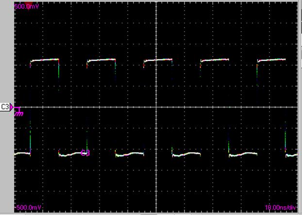
Square wave rising-edge captured on a 50GS/s scope:


Square wave rising-edge captured on a 1GS/s scope:


So, as you can see, the rising-edge of the 50MHz square wave actually is within ps (pico-second)range, but the 1GS/s scope tells you that the rising-edge takes almost 1ns (nano-second). Anyway, this is still acceptable for 50MHz square wave.

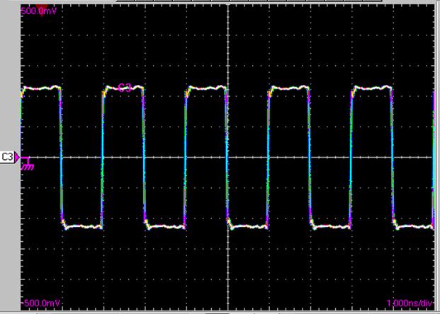
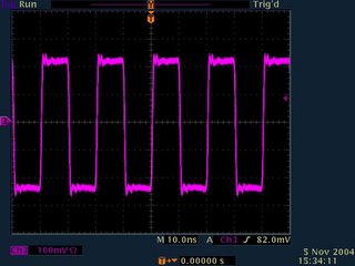
Let's now measure 250MHz square wave (also generated by FPGA) on both the 50GS/s scope and 1GS/S scope.
This is measured on the 50GS/s scope:


This is measured on the 1GS/s scope:


Needless to say, the 250MHz square wave looks more like a trapezoidal wave on the 1GS/s scope.

How does 500MHz square wave look like on both scope? Here are the scope shots.
500MHz square wave measured on 50GS/s scope:


500MHz square wave measured on 1GS/s scope and it no longer looks like square wave:


Finally, this is how the 1GHz square wave looks like on the 50GS/s and 1GS/s scope, respectively. As you can see, the 1GHz not only looks more like a sinusoidal wave from the 1GS/s scope, its amplitude is also much smaller.


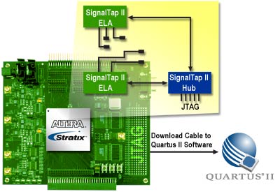
I believe all the above scope shots can prove to you the importance of bandwidth of a oscilloscope. Not only that, the bandwidth of a probe can also affect the results seen on the oscilloscope. The scope shot below is captured using a 4GHz FET probe and a SMA cable on a 7GHz storage scope. The signal measured is a 3.125Gbps signal generated by a Stratix GX FPGA device.

So, in conclusion, what are the considerations for the bandwidth? There are several rules of thumb when considering the bandwidth of an instrument.
1. Minimum bandwidth should be at least 5 times of the expected measured highest frequency.
2. If you are interested to measure the rise time, the minimum bandwidth should be 0.45/(rise time). Otherwise, the rise time that you have measured is inaccurate. For an example, look at the rise time of the 50MHz square wave captured above from different scopes.
3. Or, the minimum bandwidth is up to the 9th harmonic of the highest frequency, of course, higher the better. If you are not sure of what is 9th harmonic, then you can read my previous posts, History and Beauty of Sine Function and Building Square Wave from Fourier Series. That is the reason I said that the Fourier Series plays an important role in today's world and this is just one of the thousands examples or applications that have a close relationship with Fourier.

Tuesday, February 21, 2006

Building Square Wave from Fourier Series

As promised in my previous post, I would like to show how a square waveform can be built from the Fourier Series. I am using Tcl/Tk script to generate a periodic square wave from Fourier Series. The reason I am using Tcl/Tk language for this is because I have never practically done this before although I know it can be done. In case you haven’t heard about Tcl/Tk language before up to this point, you can read the previous post in this blog, The Interesting Tcl Language.

As you have known from my previous post, the periodic signals can be constructed using Fourier Series, which consists of summation of sine and cosine functions at frequencies which are harmonically related. The square wave function F(t) derived from Fourier Series is as follows:

F(t) = sin(t) + sin(3t)/3 + sin(5t)/5 + sin(7t)/7 + sin(9t)/9 + …
= ∑sin(nt)/n (n odd, 0< n <∞) (1.1)

It is too long to describe how the above function is derived. If you are interested to know how it is derived, it is not to difficult this information from the reference books or internet.

Since the square wave is luckily just constructed from summation of sine functions at different harmonic frequency, let’s display a simple sine wave using Tk first.

The Tcl/Tk source code for the above diagram is as follows. As you may agree, it doesn’t take many lines of complicated code to display a sine wave on your computer screen using Tcl/Tk script.

############################################
## sinewave.tcl
## date created : February 21, 2006
## author : http://fpgaforum.blogspot.com
############################################

wm focusmodel . passive
wm geometry . 460x360; update
wm resizable . 1 1
wm deiconify .
wm title . "Sine Wave Generator by FPGA FORUM"

label .msg1 -wraplength 4i -justify center -text "This generates a simple sine wave."
label .msg2 -wraplength 4i -justify center -text "http://fpgaforum.blogspot.com"
pack .msg1 -side top
pack .msg2 -side top

canvas .sinewave -bg black -width 450 -height 300
pack .sinewave

set coordList {}

#2*pi*f0 = w0 = 1/25
#fundamental frequency, f0 = 1/(25*2*pi)

for {set x 0} {$x<=450} {incr x} {
lappend coordList $x [expr sin($x/25.0) * 50 + 150]
}

eval .sinewave create line 0 150 450 150 -fill white -activefill blue
eval .sinewave create line $coordList -fill green -activefill red

##The end of sinewave.tcl
################################################


I purposely multiply the sine function result by a factor of 50 to amplify the sine wave. Otherwise, the sine wave would be too small.

The square wave, if constructed by the first 5 harmonics of sine functions looks like below. Of course, if you complain that this is not a square wave, then you are absolutely right. A perfect square wave is constructed when you have summed all the harmonics of sine functions according to the Equation 1.1.

The Tcl/Tk source code for generating the above square wave is as follows, and once again, the script doesn’t look much different from the one that generates a sine wave.

############################################
## squarewave.tcl
## date created : February 21, 2006
## author : http://fpgaforum.blogspot.com
############################################

wm focusmodel . passive
wm geometry . 460x360; update
wm resizable . 1 1
wm deiconify .
wm title . "Square Wave Generator by FPGA FORUM"

label .msg1 -wraplength 4i -justify center -text "This generates a square wave from the Fourier Series."
label .msg2 -wraplength 4i -justify center -text "http://fpgaforum.blogspot.com"
pack .msg1 -side top
pack .msg2 -side top

canvas .squarewave -bg black -width 450 -height 300
pack .squarewave

set coordList {}

#2*pi*f0 = w0 = 1/25
#fundamental frequency, f0 = 1/(25*2*pi)

for {set x 0} {$x<=450} {incr x} {
set y 0
set z 0
for {set N 1} {$N<=5} {set N [expr {$N + 2}]} {
set z [expr sin($x*$N/25.0) /$N* 50]
set y [expr $y + $z]

}
lappend coordList $x [expr $y+150]
}

eval .squarewave create line 0 150 450 150 -fill white -activefill blue
eval .squarewave create line $coordList -fill green -activefill red

##The end of squarewave.tcl
#####################################################


If the N is 101, then you can see that an almost perfect square waveform is displayed using the squarewave.tcl script. And, it is not too difficult for you to imagine that a perfect square wave will be generated if you keep on increasing the value of N, which is also the Nth harmonic sine wave from the fundamental sine wave frequency.

You may now feel curious about the real applications of the Fourier Series after reading this post. In my next post, I will tell you one real application that has the connection with what I have brought out in this post.

Sunday, February 19, 2006

History and Beauty of Sine Function


Still remember when was the first time you learn about sine function? Still remember how the sine function was derived when you were in the secondary school? I first learnt about the sine function from the trigonometry chapter at 14 years old if I remember correctly. 10 years later, I almost forgot that the sine function introduction was from a right-angled triangle. Sine function of the angle A (not the right angle) in a right angular triangle is the length of the side opposite to the angle A divided by the length of hypotenuse, which is the longest side of a right-angle triangular. Cosine function of the angle A, on the other hand, is defined as the length of the adjacent side of the angle A divided by the length of hypotenuse. From the above explanation, it is not too difficult to think that cosine function is an extension from the sine function. Perhaps this is the reason why cosine function is named as co-sine function.


Everything looks so simple when I was beginning to learn the sine and cosine functions. Never could I have thought that these simple functions have so much influence on today’s mankind history. No kidding! What would happen if there was no sine function nowadays? The influence of the sine function is too much way beyond anyone imagination.


An example of the importance of Sine function is shown obviously in Fourier Series. Fourier Series was discovered by a French mathematician, Jean Baptiste Joseph Fourier (1768-1830, one of the French Revolution contributors) when he was studying and analyzing the heat flow in a metal rod. Therefore, the Fourier Series was named in honor of him. According to the Fourier Series, a periodic function can be represented by an infinite sum of sine or cosine functions that are harmonically related. For an instance, a square wave, which doesn’t seems to be any sinusoidal at all, can be represented by a Fourier Series. (If I have the time, I would like to prove it to you in graphics next time.) If you think that this is an easy statement, then you are totally wrong. Fourier Series as well as Fourier Transform which bears his name, are considered among the greatest discoveries in scientific and engineering discipline.


There are too many periodic motions or waveforms around us all the time. To name a few, signals transmitted by the cell phone base-station, television and radio stations are sinusoidal and periodic. The alternating current (a.c.) power sources generate voltages and currents are in sinusoidal form. Function or Signal Generators generate different kind of periodic waveforms in your laboratories. The generation and analyzing of the periodic motions or waveforms are made possible through Fourier Series. Anyway, the Fourier Series will not be possible if there was no Sine function before Joseph Fourier.

Isn’t it amazing? Why sinusoidal shape matters? Why not square, triangular, or circle? This is really intriguing.

Monday, February 06, 2006

The Interesting Tcl Language


People pronounce Tcl as "Tickel". Tcl means Tool Command Language. Usually, you see Tcl paired with its young brother, Tk. Tk is the Tcl toolkit for building graphical user interfaces.
I was first introduced by this cool Tcl language about 3 years ago when I tried to find a solution to automate the compilation of Quartus II overnight and during the weekend. Basically, I had about twenty different Quartus II projects to compile and each of them took a few hours to complete due to the large logic usage and strict timing requirement inside the designs. If I didn't automate this process, I would be wasting my time to do the manual push-button compilation after every one or two hours of compilation, which was kind of stupid. So, that was my first purpose of using the Tcl language.

However, soon after that, I found out that the Tcl language is not merely a scripting language that is limited for automation process. It can do much more than that, such as file processing, easy interface with the PC serial port without any external DLL, easy construction of GUI, interface with a DLL written by you or others, etc. Besides that, I also found out that most of the FPGA tools like Quartus II, ISE and famous third-party simulation tool, ModelSim, provide the API and platform for you to command them in Tcl language.

One of the reasons people use Tcl language is that the script written in Tcl language works regardless of the operating system used. It saves the hassle of providing the software in different versions just to support different OS.
If you never heard about the Tcl and are interested with this Tcl language, you can go to ActiveState to download the ActiveTcl software, and it is freely distributed. There are many Tcl application examples that you can easily download from the website for reference. If you would like to know even more details about this cool language, you can read the Practical Programming in Tcl and Tk written by Brent B. Welch, Ken Jones with Jeffrey Hobbs. This Tcl/Tk bestseller comes with a CD-ROM that includes all the examples used in the book and also the ActiveTcl software which may have been outdated. This book (fourth edition) has been my Tcl/Tk bible since I start using Tcl and Tk and it still is.

Saturday, February 04, 2006

The Art of Prototyping


There is another huge advantage of using FPGA which I had left out in my previous post. In fact, this is one of the significant reasons the engineers are using the FPGAs. Seeing is Believing! Many IC Designers design their "designs" with simulation tools that cost them hundreds of thousand or even millions dollars, but sometimes all the simulation results before the first silicon is still not enough. So, the IC Designers work with the engineers who are familiar with the FPGA devices and tools to create a prototype for their designed IC using the RTL codes written by them. The prototype can reduce a lot of risk on the IC designed because if there is any bug found on the RTL codes, it can still be fixed, re-compiled on the FPGA tool and then verified on the FPGA again within a short period of time. As I told you in my previous post, the FPGA can be re-configured with any new design easily. In my working experience, the most impressive prototype that I had seen so far is the prototyping of a RF wireless chip in a Xilinx FPGA. Of course, the Xilinx FPGA only prototypes the digital portion of the RF chip, such as the microcontroller, JTAG (Joint-Test-Action-Group), etc.

The prototype can at least verify the functionalities of the new IC designed. But then you may ask, what is the difference between the FPGA prototype and the final product IC? Timing. It is difficult to match the timing between the FPGA and the ASIC (short form for the Application Specific IC, usually the IC designed has a specific application, such as graphics chip, USB device chip, etc) due to the different architectures inside the ASIC and the FPGA. Anyway, even if the FPGA cannot run as fast as the targetted ASIC frequency, it doesn't stop people from prototyping their final product in FPGA unless their final product is an analog device. You may also be curious, if that is the case, why don't the IC Design companies just sell their "ASICs" designs in the FPGAs? Well, the reason is simple, the cost is different. If they have the confidence that many people will love their ICs and their ASICs is going to make them a lot of money, then it is certainly very much more cost-efficient to go for ASICs. Two three years ago, FPGA vendors such as Altera and Xilinx have rolled out many low cost FPGAs such Cyclone series and Spartan series FPGAs. These low cost FPGAs certainly worth considered if the designs do not target very high frequency and high performance. However, if you are targetting the high-end FPGAs such as Stratix series or Virtex series FPGA, then you might consider selling your product with volume in ASIC because the high-end FPGAs are very expensive! Or, you may consider Altera HardCopy II as Altera promises "seamless" migration from FPGA to ASIC at NO pain!

Friday, January 27, 2006

Everybody Loves Field Programmability


If you have the choice to buy one product at the same cost, one has the upgrade ability while the other does not, most likely you will choose the former one. This is the current trend of the electronics product, which includes the big-market consumer products. More and more electronics product designers intend to put in some effort to provide the field programmability platform for their products.

Nowadays, due to the nature of the highly-competitive business world, time-to-market becomes utmost critical. If you can rollout your products faster than your competitors, your products are likely to be emerged as the product winner because your product gains the market faster than anyone else. Although your product is rolled out with the fundamental features required, the users can upgrade your product with the latest features and firmware later after purchase. This is possible if your product has the field programmability feature and this can be done using a FPGA or even CPLD. Cool huh?

Due to this reason, don’t forget to check if the electronics stuff that you are interested provides any feature upgrade ability. If you already have purchased some electronics stuff with the feature upgrade ability, then don’t miss out the latest version of features for your electronics stuff. The reason is simple; you have already paid for all the future upgradeable cool features from the moment you paid for it. Another reason you should upgrade to the latest features is the current features may have bugs and therefore don’t work well. Anyway, when you find out that the latest features fix the previous version bugs, don’t blame the engineers because the stakes is too high, the schedule is so tight and the time-to-market is getting shorter and shorter!

Actually, the field programmability is not only limited to consumer products. A very good example of the importance of field programmability is for the base station used in cell-phone communication. Base station is the radio transmitter and receiver which transmits and receives all of our calls to or from our cell-phones in a particular area (which is also called cell). We all realize that cell-phone technology upgrades very fast and the base stations just have to catch up with the latest technology used. Imagine what would happen if the base stations don't have the field programmability? I believe it would cost the telecommunication companies a lot just to keep their base stations updated with the latest features in the cell-phone technology! Just think about the base stations located high on the mountains you will know what I mean.

If you are still not sure with what I am trying to bring out here, there is a good and simple reference design for you to read, of course, provided that if you are interested to know more. This reference design targets the Altera Stratix FPGA which has the remote update configuration feature.

That’s why everybody loves field programmability!

Thursday, January 26, 2006

Soft Processor in FPGA


If you are new to FPGA, your might wonder what is the advantage of using a soft embedded processor in a FPGA. Examples of the famous soft processor in the FPGA are Altera NIOS II and Xilinx MicroBlaze. Why not using a dedicated microprocessor such as Microchip PIC microcontrollers, Motorola 68000, ColdFire or others? There are quite a number of reasons for this. Below are some that I can quickly think of.

First, you can configure as many I/Os as you desire in a FPGA as long as the FPGA chosen by you can provide that. For an example, most of the dedicated microcontrollers have the most 40 I/Os, but with a FPGA, you can have as many as 300 I/Os or even more if you are willing to pay more, and all of the I/Os can be controlled through the soft-core processor programmed in the FPGA.

Second, you can design your very own customized Intellectual Property (IP) inside the FPGA to interface with your processor. Of course, your IP would reside inside the same FPGA, too. The IP can be written in Verilog, VHDL or vendor-specific hardware description language such Altera AHDL or Xilinx XDL. For an example, in my previous post, I mentioned that I had done USB device IP cores inside FPGA. In fact, these IP cores interface with the soft-core processor inside the FPGA. The reason for having a separate IP core for some dedicated function is to have a higher performance, such as USB High Speed transfer (480Mbps) with PC. A dedicated controller alone might not act as fast as an IP core in a FPGA. For that reason, I never see any dedicated controller that supports USB High Speed transfer, at least not as far as I know. Most of the dedicated controllers only support USB transfer up to 12Mbps, which is actually the USB Full Speed transfer.

By now, you may ask, why not creating the whole design in a FPGA without the soft-core processor? Actually you can. But there are cases that you want the simplicity of writing part of your design using C/C++ code, especially those design portions that require massive processing power. See my previous post . Most of the time, using a processor helps reducing your design time and save your FPGA cost, because less logic is required if you design is relatively complicated.

Third advantage of using a soft processor in a FPGA is, you can increase your operating frequency as high as the timing requirement in your design is met. For most of the dedicated controller, you have to follow the frequency specification.

Well, enough has been said for the goods of the FPGA. Is there anything good about the dedicated microcontroller? Cost, of course! Every penny counts, you have to pay for the cool features of a FPGA!

Wednesday, January 25, 2006

C or HDL in FPGA?


There are always two options to create one design in FPGA, first through HDL and second through C language. Many FPGA beginners always ask me whether they should design their IPs in HDL or C in the FPGA. HDL, a.k.a Hardware Description Language, refers to the well-known verilog HDL or VHDL language whereas C in this article refers to the common C or C++ programming language.

If your IP needs very fast performance, it is best to design it with HDL because the design is in RTL (Register Transfer Level) and you know exactly how many clock cycles taken to transfer data among all the registers. You also define and create all the state machines needed in your IP. Using HDL, you can create as many parallel processing as possible to improve your design performance. The downside when designing with the HDL is it always takes more development and debugging time than designing with the C. Sometimes, simulation is required to make sure the HDL design behaves as expected at the targeted operating frequency.

You probably learn C language earlier than HDL in your life. So, needless to say, you most probably feel more comfortable when creating your IP in C. Besides, it always takes less development time and much easier to debug as most C compiler provides a user-friendly debugging platform. The disadvantage for C is that you can’t control much about the timing performance. You usually don’t know or you don’t even bother how much time taken to execute one function in your design. The most critical downside of C language is that you can’t do parallel processing. Everything works in serial with C, except when the DMA (Direct Memory Access) is called to work. The most you can do with C is code optimization and use the DMA as frequent as possible.

Although there are pros and cons for both design entry with HDL and C, you can actually combine both in your IP to optimize your IP performance as well as to shorten the time taken for your IP to market. For the design portion that needs critical performance, design it with HDL. On the other hand, for the design portion that requires many processing, design it with C to save some development time and also your limited logic resource in the FPGA.

In the digital world, many people refer the engineers who do their designs using HDL as Hardware Engineer whereas the engineers who write C code as Software Engineer. Many hardware-software integration issues appear due to the clear line drawn between the Hardware Engineer and Software Engineer. Due to this reason, I hate to call myself as either one of them because for me, both are just equally important.

There is a very good article that talks about the issues raised when integrating hardware and software. Feel free to read the interesting “When Hardware Met Software” from Xilinx. This is the reason I love Xilinx, they keep on publishing interesting and useful articles for public for FREE!

Tuesday, January 24, 2006

Communication Link between FPGA and PC


Nowadays, PC has become the most common platform for everybody. You use PC to store your personal data, business statistics, financial documents, digital photos, songs, etc. You also use PC to communicate daily with your family and friends through emails and messengers. For that reason, I think it is fair to say that the communication link on an embedded system with PC becomes more critical now than ever. One common example, almost all of the every recent generation of cell-phones can be connected to PC through USB.

If you have a FPGA on an embedded system, you find that at times you want your embedded system to talk to the PC. Luckily, a lot of Intellectual Properties (IP) have been designed by great FPGA companies such as Xilinx and Altera to build the connection between the FPGA and PC. Therefore, if you want to save yourself hassle from designing your own IPs, you can just buy those needed IPs from the targeted FPGA companies. Of course, these IPs are not for free but big companies certainly afford to buy the licenses for these IPs.

I personally have the experience to design and implement the communication links between a FPGA and a PC. I have designed the IP (using verilog) in the FPGA to talk to the PC via Parallel Port, Serial Port and most recently, the popular USB port. It is an wonderful feeling when I successfully communicate with the PC USB port from low-speed (1.5Mbps) to full-speed (12Mbps) using only a Cyclone FPGA and later HIGH-SPEED (480Mbps) using a Cyclone FPGA with the help of a NET2272 chip! The most difficult part when getting started is to enumerate the USB successfully. If you are already able to create an IP that can enumerate the USB device successfully with a FPGA, you are almost half way through. It is not easy but it is certainly not as difficult as you may imagine.

Monday, January 23, 2006

Hello World!

Hello World from fpga forum!

Please bookmark this forum as more interesting posts will be published for you soon!